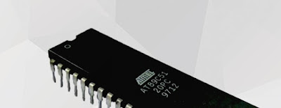
ABOUT 89C51 MICROCONTROLLER
Ø Compatible with MCS-51 Products
Ø 4 Kbytes of In-System Reprogrammable Flash Memory. Endurance 1,000 Write/Erase Cycles
Ø Fully Static Operation: 0 Hz to 24 MHz
Ø Three-Level Program Memory Lock
Ø 128 x 8-Bit Internal RAM
Ø 32 Programmable I/O Lines
Ø Two 16-Bit Timer/Counters
Ø Six Interrupt Sources
Ø Programmable Serial Channel
Ø Low Power Idle and Power Down Modes
Description:
The AT89C51 is a low-power, high-performance CMOS 8-bit microcomputer with 4 Kbytes of Flash Programmable and Erasable Read Only Memory (PEROM). The device is manufactured using Atmel’s high density nonvolatile memory technology and is compatible with the industry standard MCS-51 instruction set and pinout.
The on-chip Flash allows the program memory to be reprogrammed in-system or by a conventional nonvolatile memory programmer. By combining a versatile 8-bit CPU with Flash on a monolithic chip, the Atmel AT89C51 is a powerful microcomputer which provides a highly flexible and cost effective solution to many embedded control applications.
The AT89C51 provides the following standard features: 4Kbytes of Flash, 128 bytes of RAM, 32 I/O lines, two 16-bit timer/counters, a five vector two-level interrupt architecture, a full duplex serial port, on-chip oscillator and clock circuitry. In addition, the AT89C51 is designed with static logic for operation down to zero frequency and supports two software selectable power saving modes.
PIN Diagram :
Pin Description:
- Pins 1 to 8 − These pins are known as Port 1. This port doesn’t serve any other functions. It is internally pulled up, bi-directional I/O port.
- Pin 9 − It is a RESET pin, which is used to reset the microcontroller to its initial values.
- Pins 10 to 17 − These pins are known as Port 3. This port serves some functions like interrupts, timer input, control signals, serial communication signals RxD and TxD, etc.
- Pins 18 & 19 − These pins are used for interfacing an external crystal to get the system clock.
- Pin 20 − This pin provides the power supply to the circuit.
- Pins 21 to 28 − These pins are known as Port 2. It serves as I/O port. Higher order address bus signals are also multiplexed using this port.
- Pin 29 − This is PSEN pin which stands for Program Store Enable. It is used to read a signal from the external program memory.
- Pin 30 − This is EA pin which stands for External Access input. It is used to enable/disable the external memory interfacing.
- Pin 31 − This is ALE pin which stands for Address Latch Enable. It is used to demultiplex the address-data signal of port.
- Pins 32 to 39 − These pins are known as Port 0. It serves as I/O port. Lower order address and data bus signals are multiplexed using this port.
- Pin 40 − This pin is used to provide power supply to the circuit.
- Special Function Registers:
- Special Function Registers (SFRs) are a sort of control table used for running and monitoring the operation of the microcontroller.Even though there are 128 memory locations intended to be occupied by them, the basic core, shared by all types of 8051 microcontrollers, has only 21 such registers.
- There are 21 Special function registers (SFR) in 8051 micro controller and this includes Register A, Register B, Processor Status Word (PSW), PCON etc . There are 21 unique locations for these 21 special function registers and each of these register is of 1 byte size. Some of these special function registers are bit addressable (which means you can access 8 individual bits inside a single byte), while some others are only byte addressable.
A Register (Accumulator)
- The most important of all special function registers is Accumulator which is also known as ACC or A. It is a general-purpose register used for storing intermediate results obtained during operation.Prior to executing an instruction upon any number or operand it is necessary to store it in the accumulator first. All results obtained from arithmetical operations performed by the ALU are stored in the accumulator. Data to be moved from one register to another must go through the accumulator. In other words, the A register is the most commonly used register and it is impossible to imagine a microcontroller without it.
- ACC is usually accessed by direct addressing and its physical address is E0H. Accumulator is both byte and bit addressable. You can understand this from the figure shown below. To access the first bit (i.e bit 0) or to access accumulator as a single byte (all 8 bits at once), you may use the same physical address E0H. Now if you want to access the second bit (i.e bit 1), you may use E1H and for third bit E2H and so on.
-
B Register
- Multiplication and division can be performed only upon numbers stored in the A and B registers. All other instructions in the program can use this register as a spare accumulator(A).The 8051 micro controller has a single instruction for multiplication (MUL) and division (DIV).
- Eg: MUL A,B – When this instruction is executed, data inside A and data inside B is multiplied and answer is stored in A.
- Note: For MUL and DIV instructions, it is necessary that the two operands must be in A and B.
Program Status Word (PSW) Register
- PSW register is one of the most important SFRs. It contains several status bits that reflect the current state of the CPU. Besides, this register contains Carry bit, Auxiliary Carry, two register bank select bits, Overflow flag, parity bit and user-definable status flag.
CY, the carry flag
- This flag is set whenever there is a carry out from the D7 bit.
- This flag bit is affected after an 8-bit addition or subtraction.
- It can also be set to 1 or 0 directly by an instruction such as “SETB C” and “CLR C”where “SETB C” stands for “set bit carry” and “CLR C” for “clear carry”.
AC, the auxiliary carry flag
- If there is a carry from D3 to D4 during an ADD or SUB operation, this bit is set; otherwise, it is cleared.
- This flag is used by instructions that perform BCD (binary coded decimal) arithmetic.
- The parity flag reflects the number of 1 s in the A (accumulator) register only. If the A register contains an odd number of Is, then P = 1. Therefore, P = 0 if A has an even number of 1s.
OV, the overflow flag
- This flag is set whenever the result of a signed number operation is too large, causing the high-order bit to overflow into the sign bit.
- In general, the carry flag is used to detect errors in unsigned arithmetic operations.
- The overflow flag is only used to detect errors in signed arithmetic operations


Comments
Post a Comment